
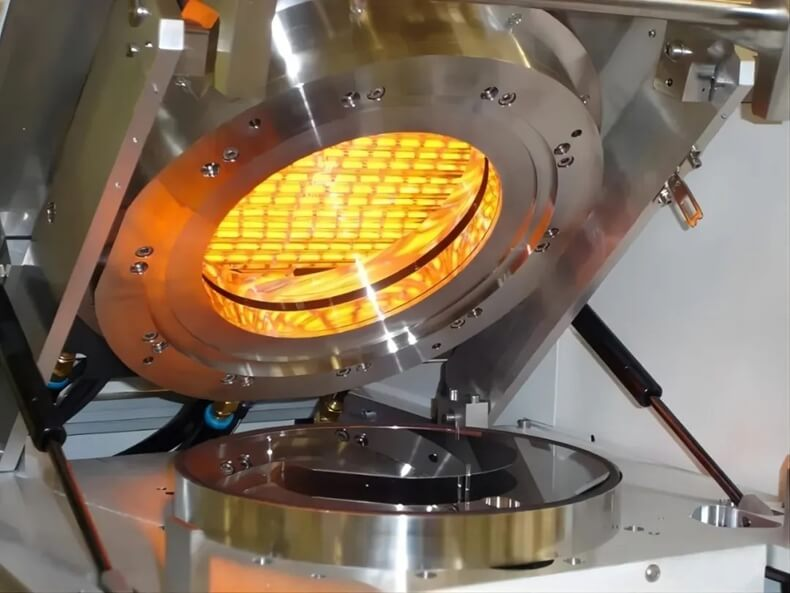
On the lithography floor, a 0.5°C drift during soft bake isn’t a small error. It’s a scrapped lot. We built our semiconductor heater components in China to keep thermal behavior inside the process window—hour after hour, shift after shift. What matters, technically We spec halogen lamp modules with short-wave and medium-wave options, so you can match photoresist absorption and the thermal budget. Wafer-level uniformity stays at ±0.1°C, measured on-tool with calibrated sensors. The heater body uses quartz and high-purity ceramics—chosen for low outgassing and zero particle generation in Class 1–100 cleanroom conditions. Power density is tuned for a fast ramp and a stable plateau, so soft bake and hard bake profiles repeat within tight tolerances. Interfaces are designed to fit standard tool footprints, with solid connectors and shielded wiring to keep signal integrity and EMI under control. Here’s the thing: in photoresist processing, temperature repeatability is what drives critical dimension control and keeps defect performance in line. Our heaters stabilize the bake profile, cut down rework, and keep the line moving. Energy use comes down because the radiant transfer is efficient and the thermal design is smart. Reliability shows up in 24/7 operation—units run 5,000+ hours with less than 5% output drop. For wafer cleaning and drying, consistent heating keeps surface energy and drying kinetics repeatable, so you don’t get yield excursions tied to thermal variability. The short version? These heaters work with most wafer track and coat/bake platforms, but integration has to match the tool’s airflow, clamping, and sensor locations. Expect a short commissioning window to nail profile offsets and cleanroom validation. But there’s one constraint you can’t ignore: dense packaging can make service access tight. Plan maintenance around scheduled lamp replacement and thermal window verification.